
Understanding cliff layer semiconductor and their functions
Anúncios
A cliff layer semiconductor is a special type of semiconductor material that has been designed to resist radiation damage. This material is able to withstand high doses of radiation without being damaged, making it ideal for use in devices that are exposed to high levels of radiation. Cliff layer semiconductors are made from a variety of materials, including silicon, germanium, and silicon-germanium alloys. These materials are carefully chosen for their ability to resist radiation damage, and they are often used in conjunction with other materials to create a more durable device. Cliff layer semiconductors are an important part of many modern devices, and they are constantly being improved to better resist the damaging effects of radiation.
A few years ago, a new type of semiconductor called cliff layer semiconductor (CLS) was developed. This new type of semiconductor is made by depositing thin layers of material on top of each other, like building a wall. The result is a much cheaper and more efficient way to make semiconductors.
Anúncios
How cliff layer semiconductor Works
CLS works by depositing thin layers of material on top of each other. The result is a much cheaper and more efficient way to make semiconductors. The first step in the process is to deposit a thin layer of material, usually silicon, onto a substrate. This substrate can be anything from glass to sapphire. The next step is to add another layer of material on top of the first layer. This second layer can be made of any number of materials, including germanium, indium arsenide, or even carbon nanotubes.
Anúncios
The third and final step is to add an insulating material on top of the second layer. This insulating material prevents the current from flowing between the two layers and prevents electrical shorts. Once the insulating material is in place, the final product is complete. Cliff Layer Semiconductors have many advantages over traditional semiconductors. They are cheaper to produce, more efficient, and can be made in any size or shape.
What is Cliff Layer Semiconductor?
Cliff layer semiconductor is a type of semiconductor material that is used in the fabrication of integrated circuits (ICs). It is made up of two or more thin layers of semiconductor material, typically silicon, that are separated by a thin layer of insulating material. Cliff layer semiconductors have a number of advantages over traditional single-layer semiconductor materials. They are easier to fabricate, have a higher degree of flexibility, and can be used to create a wide range of circuit designs.
What is a Cliff Layer?
A cliff layer is a thin sheet of material, typically just a few atoms thick, that is used to create electrical connections between semiconductor devices. Cliff layers are often made from conducting metals such as copper or aluminum, and they are used in a variety of semiconductor devices, including solar cells, LED lights, and transistors.
What are the benefits of Cliff Layer Semiconductor?
Cliff Layer Semiconductor (CLS) is a type of semiconductor that has many benefits over traditional silicon-based semiconductors. CLS is much more resistant to radiation and has a higher breakdown voltage, which means it can withstand higher voltages without breaking down. Additionally, CLS is less likely to suffer from latch-up, meaning it can be used in a wider variety of applications. Finally, CLS can be manufactured using standard semiconductor manufacturing processes, making it easier and less expensive to produce than other types of semiconductors.
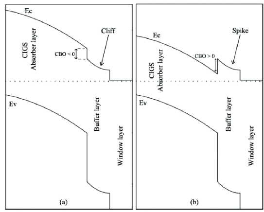
What is CIGs solar cell processing
The thin-film solar cell fabrication process starts with the deposition of the back contact layer on a substrate. Because this component plays an important role in the electrical and structural properties of the cells, it is crucial to maintain a specific setup and use compatible processes to create it. The most common deposition method for back contact layers is evaporation or sputtering and they should be used when depositing molybdenum (Mo).
What are Lateral layered semiconductors?
Layered semiconductors, represented by transition metal dichalcogenides (TMDCs), have long captured the attention of the scientific community thanks to their unique and tunable electrical and optical properties. In particular, lateral layered semiconductor multi junctions, including homojunction, heterojunctions, hybrid junctions, and superlattices – present a totally new degree of freedom in high-performance device research beyond traditional materials and their structures. However, advances in this field are limited by the precise synthesis of high-quality connections and greatly hampered by ambiguous device performance limits. Herein we review the recent key breakthroughs in the design and optimization of lateral semiconductor multijunction along with their application-specific devices. Specifically, the synthesis methods based on different principles (chemical and external source-induced methods) are introduced stepwise for the controllable fabrication of semiconductor multijunction as the basics of device application. Subsequently they’re structurally modulated according to electronic structures, exciton dynamics and optical properties before the fabrication of lateral layered semiconductor multimers. Precise property control will result in outstanding device performances: high-quality diodes and FETs; scalable logic or analog circuits; highly efficient optoelectronic
Conclusion
A cliff layer semiconductor is a type of semiconductor that is made up of a cliff-like structure. The cliff layer structure is made up of alternating layers of materials, typically silicon and another material, such as germanium. The cliff layer semiconductor has a number of advantages over other types of semiconductors, including a higher degree of control over the electrical properties of the device. In addition, cliff layer semiconductors are less likely to suffer from defects and can be made with a lower level of impurities. As a result, cliff layer semiconductors are often used in high-end electronic devices, such as cancer treatment machines and satellite communications equipment.
")


