
Cliff Layer Semiconductor (Explained in simple terms)
Anúncios
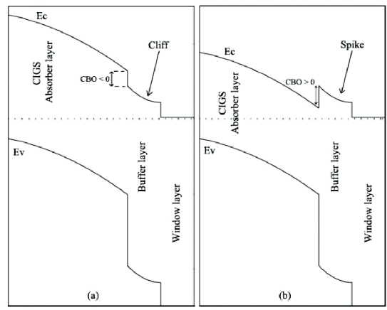
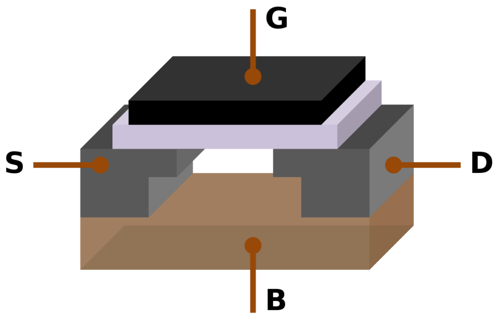
Image from researchgate
A cliff layer semiconductor (CLSC) is a section within a semiconductor device in which the active region is suspended over a cliff or ledge. You will usually find it between the band alignment of the absorber and the buffer layer. The term “cliff” refers to the sharply sloped side of the active region, while the “ledge” is the relatively flat top surface. Cliff Layer semiconductors are typically fabricated using silicon-on-insulator (SOI) technology, in which a thin layer of silicon is deposited on an insulating substrate. The active region is then patterned and etched to create the cliff and ledge structure.
Anúncios
Functions of cliff layer semiconductor
Compared to conventional planar semiconductors, Cliff Layer Semiconductor offers several advantages.
- The cliff layer serves as a barricade which then blocks injected electrons at forward bias, resulting in the recombination of majority carriers
- Another important function is that the cliff provides electrical isolation between the active region and the rest of the device, allowing for higher packing densities and improved device performance.
- In addition, the use of SOI technology enables the fabrication of very thin devices, which are essential for applications such as optical communications and high-speed digital electronics.
what is Inversion layer semiconductor?
Inversion layer semiconductors are semiconductors that have holes in them. They are formed when electrons from the emitter are injected into the collector region. This causes a virtual p-n junction to be pinched off, resulting in the characteristic transistor action. This type of semiconductor can achieve up to 45 mA mm-1 at three V base voltage thanks to an enhanced tunneling mechanism.
Anúncios
Inversion layer semiconductors are typically formed when the gate voltage is more positive than the surface potential of the semiconductor. The depletion layer width increases exponentially as the gate voltage increases. At these higher voltages, the electrons in the semiconductor become free. Inversion layer semiconductors are a common type of semiconductor.
One of the major advantages of inversion layer semiconductors is that they can withstand high temperatures and crystal damage. MIS is a process that uses a diffused metal grid that contacts the semiconductor inversion layer. MIS cells have high efficiency and are ideal for high-quality materials. Another advantage of MIS cells is that they are ideal for high-efficiency solar cells.
An inversion layer is created on a silicon surface. It is formed by an electric field and forms the basis for the operation of surface controlled devices such as the charge-coupled device, metal-oxide-silicon field effect transistor, and metal-nitride-oxide silicon memory transistor. Because the inversion layer is electrically decoupled from the bulk silicon, its characteristics are favorable for studying transport phenomena. Further, it can be controlled by electrically controlling the concentration of carriers or Fermi energy.
The most basic characterization method of inversion layer semiconductors was by conducting capacitance-voltage measurements. This method showed that the depletion region of the HCAP corresponded to the depletion region of the HCAP. By using this technique, researchers were able to establish the depletion region of p-Si and observed the formation of an inversion layer. This resulted in an improvement of the performance of NHCAP devices.
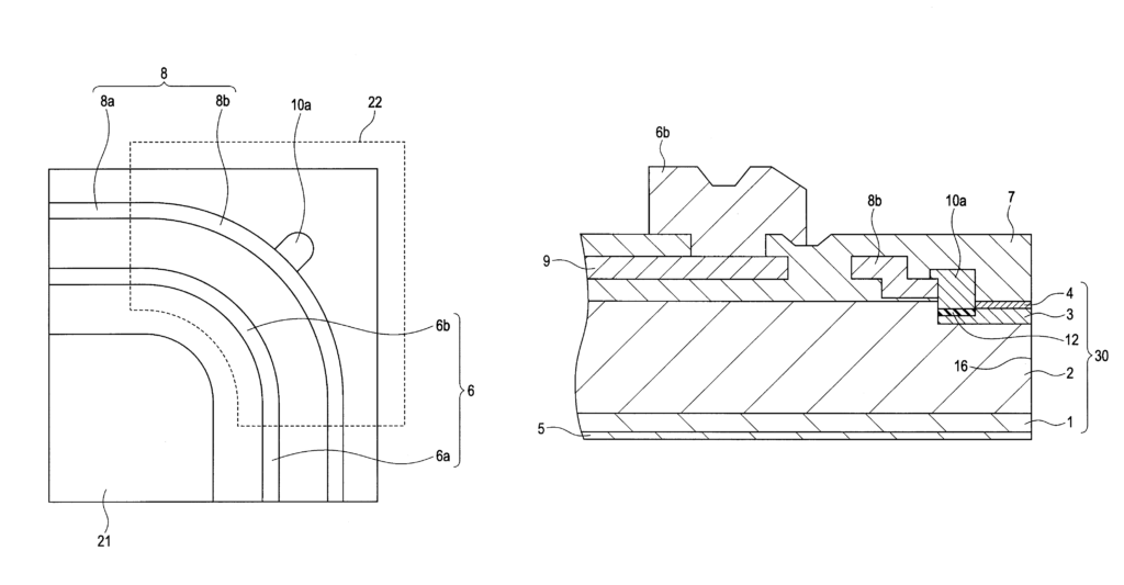
N-type cliff layer semiconductor
An N-type cliff layer semiconductor is a semiconductor with an extra layer of electrons.
According to the authors of this research, at the point where the CBO is negative and the location of the CBM of the n-type semiconductor is lower than that of the p-type semiconductor, it will create a cliff-like band alignment, causing enhanced carrier recombination at trap states. This barrier at heterointerfaces results in the recombination of majority carriers against injected electrons
These electrons are located on the p-side of the semiconductor. This is because of atoms on the p-side need holes. These extra electrons migrate across the p-n junction and create an electric potential. This electric potential prevents further charge carriers from moving. When this happens, there are no more free carriers in the layer.
Usage of N-type cliff layers
N-type cliff layers are commonly used for power-related applications. They provide high-performance devices with high-efficiency and low-power consumption. These devices are typically made with two layers. The lower-energy region is a thin layer of N-type semiconductor, while the upper layer contains a higher-density region of Ge.
The p-side of a N-type cliff layer semiconductor is formed with a ring-like side wall. This layer is connected to the driving power supply and to a p-side ohmic electrode. A p-side ohmic electrode is placed over the ring-like portion.
Source:https://patents.google.com/patent/US9263280B2/en
The semiconductor light-receiving device is comprised of a semi-insulating substrate and upper, middle, and lower regions. The lower region has a p-type first layer with a top surface on level with the middle region. A second semiconductor layer is provided on top of the p-type semiconductor layer. This second layer has a bottom surface.
In a N-type cliff layer semiconductor, one or more impurities donate electrons to the lattice. The excess electrons are known as n-type dopants. In such a material, electrons outnumber holes, making them the majority carriers.
An N-type cliff layer semiconductor is an important material for making transistors. Its properties include high conductivity and high stability. However, it must be noted that the layers may be prone to degradation during manufacturing. The semiconductors should be tested under conditions that will minimize the risk of defects.
what is the Channel region between gate dielectric and buried oxide region?
The channel region between the gate dielectric and buried oxide region in a Cliff layer semiconductor is a thin film that extends between the source and drain. A voltage applied across the gate controls the channel’s conductivity. A greater voltage will allow more current to flow from the source to the drain. This effect is called enhancement mode.
A channel formed in a semiconductor device is called a MOSFET. Its channel region is extremely thin. The source and drain regions are formed in an additional layer above the channel. The two additional terminals, which connect the two highly doped regions are the same or opposite in type to the body region.
This channel is usually silicon, but in recent years, companies have started to use the SiGe alloy as a channel material for MOSFETs. However, gallium arsenide is not suitable for MOSFETs because it does not form a good semiconductor-to-insulator interface.
Creating an isolated silicon island in a Cliff layer semiconductor
- The first method of creating an isolated silicon island in a Cliff layer semiconductor is to cover the channel region with silicon nitride. Then, oxidizing the surface of the semiconductor body can result in the formation of islands of silicon.
- The second method of creating silicon in a Cliff layer semiconductor is to use an anisotropic etching process. During the etching process, silicon is selectively removed from regions adjacent to the polysilicon gates. During this step, silicon must be prevented from growing oxide.
- The third method for creating transistors using Cliff layer semiconductors is to use a trench structure. A trench is a patterned region formed by a single layer of silicon. This region is the common drain/source region in two S/DOI transistors.
Using ISE-TCAD, we designed thin S/D bFDSOI-FETs. Next, we deposited a 60-nm layer of oxide using chemical vapor deposition as a blocking layer. Once that layer was etched away, we then deposited poly-Si to form the active layer.
Manufacturability of cliff layer semiconductor
A critical factor in the manufacturability of a semiconductor is the distance between the cliffs. The further apart the cliffs are, the narrower the passage between them will be. This is a fundamental problem that must be resolved by the litho-community.
Fortunately, many governments have taken a proactive role in supporting local semiconductor industry development. By setting regulations that encourage growth, providing financial support, and creating an environment that attracts talent, governments are making it easier for local semiconductor companies to grow. However, government policies have often changed over the years, and the semiconductor industry has been negatively affected by the tightening of immigration policies. However, the semiconductor industry has recently noticed a resurgence in government support. Some governments have even launched new subsidies to attract local semiconductor companies.
Conclusion
A cliff layer semiconductor is a type of semiconductor that is made up of two layers of materials that are separated by a thin gap. One of the layers is typically made of silicon, while the other layer is made of another material such as germanium. The two layers are separated by a very thin insulating layer, which prevents the flow of electrons between the two layers. The size of the gap between the two layers determines the type of semiconductor: if the gap is small, it is called an N-type semiconductor, and if the gap is large, it is called a P-type semiconductor. Cliff layer semiconductors are used in a variety of electronic devices, including transistors and solar cells.
References and sources
https://pubs.rsc.org/en/content/articlelanding/2022/cs/d1cs01092a
Energy band alignment at the heterointerface between CdS and Ag-alloyed CZTS | Scientific Reports


